PCBs are an essential component in the development of electronic devices, providing a way to interconnect and control various electronic components. The process of designing a PCB can be complex and requires careful consideration of various factors such as component placement, trace routing, and copper pouring. In this blog post, we will walk you through the step-by-step process of designing a PCB, from creating a schematic design to generating the Gerber files. Whether you are a beginner or an experienced designer, this post will provide you with valuable insights into designing a high-quality PCB. So let’s get started!
What is a PCB?
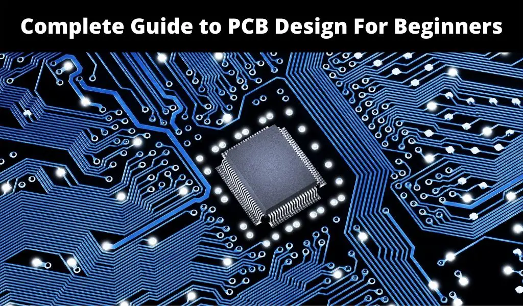
A printed circuit board (PCB) is a board made of insulating material, such as fiberglass or plastic, that is used to connect electronic components such as integrated circuits (IC), resistors, capacitors, inductors, diodes, and connectors using conductive pathways or traces. The conductive traces are usually made of copper, which is etched onto the board in a specific pattern that allows for the interconnection of these components. PCBs come in various shapes, sizes, and designs, and can be single-sided, double-sided, or even multi-layered, depending on the complexity of the circuit design. They are widely used in electronic devices such as smartphones, computers, televisions, appliances, and many others.
Parts of a PCB
PCBs can have different layers depending on the complexity of the circuit design. A simple PCB may only have one or two layers, while more complex PCBs can have up to 16 or more layers. The layers of a PCB include the top and bottom layer, signal layers, power and ground planes, silkscreen, and solder mask.
- Top Layer: This is the topmost layer of the PCB, where most of the components are placed and connected.
- Bottom Layer: This is the bottom layer of the PCB, where the remaining components are placed and connected. Components can only be placed on the top or bottom layers.
- Substrate: The substrate is typically made of an insulating material such as fiberglass, epoxy resin, or a composite material. It serves as the foundation for the entire PCB, and its properties can affect the performance and reliability of the final product. The substrate must be able to withstand the temperature, pressure, and environmental conditions that the PCB will be subjected to during its lifetime. Furthermore, it keeps insulated adjacent copper layers so they don’t short together.
- Signal Layers: These layers contain the conductive traces that connect the components on the board. A typical PCB can have two to eight signal layers, depending on the complexity of the circuit design.
- Solder Mask: is the PCB’s protective skin. It is made of polymer and is meant to shield the copper layer from short circuits when it comes into contact with the environment.
- Silkscreen: This layer contains markings and labels that help identify the components and their placement on the PCB. This is mainly used for assembly so that you’re able to figure out which part goes where.
Luckily, most of us who use electronic devices don’t have to worry about what’s under the hood for PCBs. However, if you are an electronic engineer like us, knowing about PCBs is a necessity. There’s a lot to learn and it could take years to become an expert.
PCB Design
If you have all the parts for the circuitry you are designing, but are lacking the PCB, your device is as good as nonexistent. The PCB design process brings your device to life. There are several steps involved in designing a PCB, and we will walk through each step in detail. Before reading on, it might be worthwhile to check out our blog post on the different PCB design software that is available to use for free!
Step 1: Schematic Design
The first step is to actually design the schematics for all the circuits that will going on the board. The schematic is a graphical representation of the components and connections in a circuit. This could be circuits for power regulation and protection, LEDs, comparators, operational amplifiers, clocks, controllers, etc. The software usually comes with a library that has components that you can use in your schematic, but sometimes you’ll have to create the components yourself.
Step 2: Layout
Once the schematic is complete, the next step is to create a PCB layout design. The PCB layout is the physical representation of the circuit board. This includes the placement of components, the routing of traces, and the placement of vias and holes.
When designing the layout, it’s important to consider the size and shape of the PCB, the number and type of components, and the routing of traces. The layout should be optimized for maximum efficiency and ease of manufacturing. You should also try to group components together based on their functionality and minimize the length of the traces between them.
Step 3: Trace Routing
Trace routing is the process of connecting components on the PCB with copper traces. When routing traces, you need to consider factors such as signal integrity, power consumption, and electromagnetic interference (EMI). You should also avoid crossing traces and keep them as short as possible. If you find that crossing traces is inevitable then you’ll need to add more signal layers to your board stackup (more on this in Step 4). There are entire books written on signal routing. This comes with practice and years of experience to design the most optimal routing.
Step 4: Defining the Layer Stackup
The layer stackup is an important part of the PCB design process, as it determines the number and order of the layers in the final PCB. The layer stackup is chosen based on the requirements of the circuit design, the number of signal layers needed, and the manufacturing process.
The layer stackup specifies the order of the layers and the thickness of each layer, which affects the overall thickness of the PCB. For example, you can specify heavier copper or a different substrate based on your application. The layer stackup also determines the placement of the power and ground planes which can affect the electromagnetic compatibility (EMC) and signal integrity of the circuit.
Step 5: Copper Pour
Copper pouring is the process of filling unused areas of the PCB with copper to create a solid ground or power plane. This helps to reduce EMI and improves the overall performance of the circuit. You should try not to route signals on these layers so that you have unbroken planes.
Step 6: Drill Holes
Marking holes for drilling is a critical step in the PCB design process, as it determines the location of the holes for mounting and connecting components. Marking the holes correctly is essential for ensuring that the components fit properly on the PCB and that the connections are made accurately. You can also use the drill holes to mount the PCB to something or use them for standoffs so you can easily test the board once it’s assembled.
Step 7: Design Verification
Before sending the PCB design to manufacturing, it’s important to verify that nothing violates the default rules or custom rules that you create. Rules can be something like specifying the minimum trace width, minimum hole size, or minimum clearances between vias and a trace width.
Step 8: Gerber File Generation
The final step in designing a PCB is to generate the Gerber files. Gerber files are the standard file format used in the PCB manufacturing process. They contain all the information needed to produce the PCB, including the component placement, trace routing, and copper pouring.
Conclusion
The comprehensive process for PCB design can sound complex for beginners and we hope that we didn’t scare you away! Mastering each step comes with practice and years of experience, but it’s all worth it once you get your PCBs back from the manufacturer!


